


Inside the 8085: The Microprocessor Architecture That Changed Computing Forever!
This guide walks you through the essential internal components and workings of the Intel 8085 microprocessor. You’ll learn how its architecture operates, why it mattered in early computing, and how its efficient design still informs modern processor engineering.
Table of Contents
- Architecture Overview
- Register Organization
- ALU and Flag Register
- Buses and Control Unit
- Instruction Execution Cycle
- Applications and Historical Impact
- Top 5 Frequently Asked Questions
- Final Thoughts
- Resources
Architecture Overview
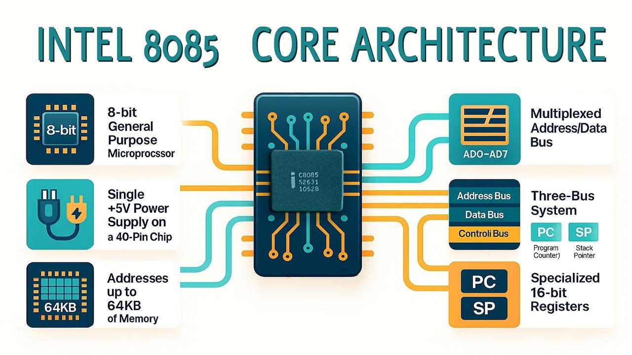
The 8085 microprocessor, introduced by Intel in 1976, is an 8-bit CPU built on NMOS technology. Its name “8085” reflects its compatibility with the earlier 8080, while adding internal enhancements like a built-in clock generator and system controller. The processor operates at 3 MHz, executes nearly 80 instructions, and supports around 246 opcodes.
Its architecture revolves around five main elements:
- a programmable register block
- the Arithmetic Logic Unit (ALU)
- the system buses (address, data, and control)
- a control and timing unit
- a flag register for decision-making logic
This architecture made it small, cost-effective, and perfect for embedded systems and educational use.
Register Organization
The register organization of the 8085 forms the backbone of its processing capability. The design follows a highly structured model to support arithmetic operations, memory interactions, and efficient instruction execution.
General-Purpose Registers
The processor provides six general-purpose registers: B, C, D, E, H, and L. Each register is 8 bits but can be paired to form 16-bit register pairs—BC, DE, and HL. These pairs allow the microprocessor to operate on 16-bit memory addresses or execute 16-bit arithmetic.
- BC pair: Often used for looping counters and data movement
- DE pair: Used for intermediate data storage and peripheral I/O operations
- HL pair: Known as the “memory pointer” since it frequently stores memory addresses
This pairing technique is a major reason the 8085 maintained strong performance despite being an 8-bit processor.
Special-Purpose Registers
Different tasks require dedicated registers to maintain control-flow integrity and operational accuracy.
- Accumulator (A):
The heart of 8085 arithmetic and logic processing. All operations pass through it, forming the bridge between the ALU and the bus system. - Program Counter (PC):
A 16-bit register that keeps track of the next instruction’s memory address. After every fetch, the PC auto-increments to maintain sequential execution unless a jump or call instruction alters control flow. - Stack Pointer (SP):
Another 16-bit register pointing to the top of stack memory. It plays a critical role in subroutine calls, interrupt handling, and local variable storage. - Instruction Register (IR):
Temporarily holds the opcode of the current instruction. While not programmer-accessible, it ensures the processor decodes and executes operations correctly.
ALU and Flag Register
The Arithmetic Logic Unit (ALU) handles addition, subtraction, logical AND/OR/XOR, increments, decrements, and complement operations. It works closely with the flag register, which contains five condition flags:
- Zero (Z): Set when the result of an operation is zero
- Sign (S): Mirrors the MSB, indicating positive or negative outcomes
- Parity (P): Set when the result contains even parity
- Carry (CY): Set when an operation generates a carry or borrow
- Auxiliary Carry (AC): Supports BCD (Binary-Coded Decimal) operations
These flags allow the processor to make decisions through conditional jumps—essential for loops, branching, and comparisons.
Buses and Control Unit
The 8085 communicates internally and externally using three main buses:
Address Bus (16-bit):
Carries memory addresses, allowing access to 64 KB of memory space.
Data Bus (8-bit):
Bidirectional, used to transfer instruction bytes and data values.
Control Bus:
Includes signals such as RD, WR, IO/M, and ALE that manage read/write cycles, memory/I/O selection, and timing.
At the center of all coordination lies the Control and Timing Unit, which:
- synchronizes operations using the internal clock generator
- decodes opcodes to trigger internal processes
- manages machine cycles and T-states
- ensures precise data flow between internal and external components
This combination allows the 8085 to execute each instruction reliably in a predictable number of cycles—an essential trait in embedded systems.
Instruction Execution Cycle
Understanding the instruction execution process reveals how efficiently the 8085 uses its architecture.
Every instruction passes through three primary phases:
- Fetch Phase:
The Program Counter places the memory address on the address bus, the opcode is fetched, and the PC increments. - Decode Phase:
The Instruction Register feeds the opcode into the decoder, mapping it to the appropriate internal control signals. - Execute Phase:
Depending on the instruction, the ALU calculates results, registers are modified, memory is accessed, or control-flows change.
Each operation is broken into machine cycles (opcode fetch, memory read, memory write, I/O read/write), and each machine cycle contains several T-states (clock cycles). This precise breakdown allows engineers to estimate performance and optimize program timing.
Applications and Historical Impact
The 8085 had enormous influence during the late 1970s and early 1980s. Its low cost, ease of integration, and approachable instruction set made it a leading choice for:
- early home computers
- communication devices
- industrial controllers
- robotics systems
- digital instrumentation
- academic microprocessor training kits
Its predictable timing, stable electrical characteristics, and clear documentation made it invaluable for system designers. Even though modern processors operate at vastly higher performance levels, the 8085 remains a foundation for understanding microprocessor design principles such as pipelining, memory mapping, and bus arbitration.
Top 5 Frequently Asked Questions
Final Thoughts
The 8085 is far more than an early microprocessor—it’s a timeless teaching tool and an engineering milestone. Its architecture demonstrates how efficient design can deliver reliable performance with minimal hardware overhead. The balance between simplicity and capability makes it an essential reference point for students and professionals exploring embedded systems, processor design, and low-level computing. Understanding what happens “inside the 8085” provides insight into how modern CPUs evolved and why foundational concepts like registers, buses, and timing cycles remain universal.


Leave A Comment